
The modern artificial intelligence revolution is driven by the semiconductor industry—a sector flooded with dense jargon like CPU, GPU, HBM, and Foundry. Yet beneath this complex global infrastructure lies a surprisingly clear and logical division of labor.
How can a silicon chip no larger than a fingernail mimic human intelligence and power multi-billion-dollar data centers or interplanetary spacecraft? Semiconductors are not just electronic components; they are the physical manifestation of digital cause-and-effect. This guide breaks down the core terms, component workflows, and strategic battles between global market leaders and emerging challengers.
1. Core Terminology Guide
- CPU (Central Processing Unit): The “brain” of a computer. A versatile processor designed for sequential, high-speed execution of complex logic and general-purpose tasks. (e.g., Intel Core, AMD Ryzen)
- GPU (Graphics Processing Unit): A specialized processor built to execute massive parallel calculations simultaneously. Originally created for 3D graphics, it has evolved into the foundational engine for AI deep learning. (e.g., NVIDIA H100, Blackwell)
- DRAM (Dynamic Random-Access Memory): High-speed volatile memory that loses stored data when powered off. It serves as an ultra-fast temporary workspace for CPUs and GPUs.
- HBM (High Bandwidth Memory): An advanced memory architecture made by vertically stacking multiple DRAM dies using 3D integration. It expands data transfer pathways, solving the memory bottleneck in AI GPUs.
- NAND Flash: Non-volatile storage that retains data without power. It acts as a long-term warehouse for massive volumes of enterprise data. (e.g., Solid-State Drives / SSDs)
- Legacy Semiconductors: Microchips produced using mature manufacturing processes (typically 28nm or older). They are foundational components across automotive, home appliance, and consumer electronics industries.
- Foundry: Pure-play contract manufacturers that fabricate silicon wafers based on proprietary schematics provided by design-only companies. (e.g., TSMC)
- Advanced Packaging: Post-fabrication technology that integrates multiple distinct chips—such as GPUs and HBM modules—into a single high-performance system. (e.g., TSMC CoWoS)
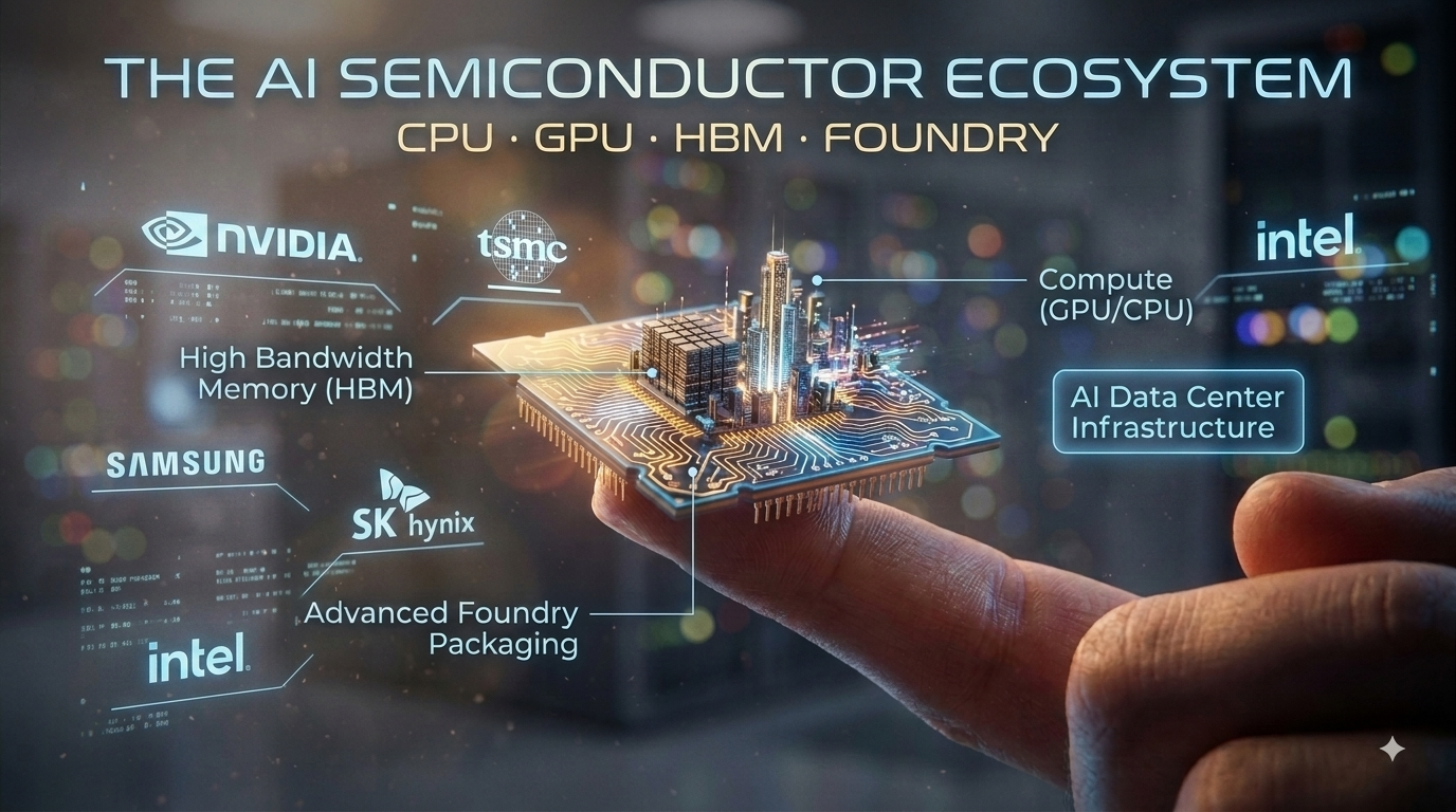
2. Analogical Framework: The AI Semiconductor Ecosystem
To visualize how these components interact, imagine an AI data center as a massive, state-of-the-art fulfillment center.
| Category | Product / Tech | Analogy & Role | Remarks |
|---|---|---|---|
| Compute (Brain) | CPU | Versatile general manager (handles complex decision-making & overall control) | Sequential computing specialized |
| GPU | Thousands of simple calculation workers (processes massive AI workloads simultaneously) | Parallel computing specialized | |
| Memory | DRAM | Small, fast personal desk (holds active working data) | Volatile / High-speed |
| HBM | Ultra-fast data tube right next to the desk (instantly feeds massive data to GPU) | 3D Stacked DRAM Architecture | |
| NAND | Large data warehouse (stores high-volume data long-term before/after processing) | Non-volatile / High-capacity | |
| Manufacturing (Making) | Foundry | Custom manufacturing plant producing state-of-the-art chips | Contract manufacturing |
| Packaging | Technology that perfectly packages and connects multiple chips into a single unit | Key to performance enhancement |
3. Four-Stage Supply Chain Workflow
Before an AI chip powers a enterprise server, it moves through a highly specialized four-stage global value chain:
- IP & EDA (Design Tools & Intellectual Property): Vendors like ARM, Synopsys, and Cadence provide critical software suites and core architectural IP that serve as the foundation for modern chip design.
- Fabless (Design Specialists): Companies such as NVIDIA, AMD, and Apple design sophisticated System-on-Chip (SoC) architectures tailored to market needs without operating physical factories.
- Foundry (Front-End Manufacturing): Pure-play fabricators like TSMC and Samsung Electronics print microscopic circuitry onto silicon wafers using nanometer-scale photolithography.
- Advanced Packaging & OSAT (Back-End Assembly): Post-fabrication facilities bond raw silicon dies with high-speed memory modules, test structural integrity, and assemble final commercial processors.
4. Key Global Players & Strategic Outlook
1) NVIDIA (United States) — The AI Ecosystem Leader
- Market Position: Commands an estimated 80% to 90% share of the global AI accelerator market.
- Key Strengths: Industry-leading GPU performance backed by CUDA, a proprietary software platform that creates high switching costs for developers.
- Vulnerabilities: Heavy dependence on TSMC’s advanced packaging capacity (CoWoS) creates supply bottlenecks. Facing growing pressure from hyperscalers developing custom ASIC chips.
- Near-Term Strategy: Scaling production of the Blackwell architecture while expanding from standalone GPU sales into full-stack data center infrastructure.
2) TSMC (Taiwan) — The Premier Pure-Play Foundry
- Market Position: Dominates advanced semiconductor manufacturing with over 70% foundry market share.
- Key Strengths: High manufacturing yields, leading 3nm and 2nm node capabilities, robust advanced packaging infrastructure, and a strict policy of never competing with customers.
- Vulnerabilities: Geographic exposure to geopolitical tensions in the Taiwan Strait, alongside operational complexities as it builds facilities in the U.S., Japan, and Europe.
- Near-Term Strategy: Commercializing its 2nm Gate-All-Around (GAA) process node while diversifying production via international fabrication expansion.
3) Samsung Electronics (South Korea) — The Integrated IDM Giant
- Market Position: Holds the leading share in global DRAM (~38%) and ranks second in contract foundry manufacturing.
- Key Strengths: Unique status as an Integrated Device Manufacturer capable of offering turnkey solutions spanning memory, foundry, and packaging.
- Vulnerabilities: Yield stabilization challenges at leading-edge nodes, wider market share gaps compared to TSMC, and qualification delays in early HBM cycles.
- Near-Term Strategy: Securing market leadership in 6th-generation HBM (HBM4) and improving yields on advanced foundry nodes to attract tier-one customers.
4) SK Hynix (South Korea) — The HBM Pioneer
- Market Position: Holds the top market position in high-bandwidth memory (>50% share in HBM) and ranks second overall in global DRAM.
- Key Strengths: Proprietary Mass Reflow Molded Underfill (MR-MUF) technology delivering superior thermal management and yield stability, backed by a strong strategic partnership with NVIDIA.
- Vulnerabilities: High exposure to memory industry supply cycles; lack of an internal pure-play foundry division.
- Near-Term Strategy: Expanding supply of HBM3E modules and collaborating with TSMC to develop custom HBM4 solutions.
5) Micron Technology (United States) — The Agile Memory Contender
- Market Position: Ranks third in global DRAM (~20–22%) and holds roughly 20% market share in specialized HBM.
- Key Strengths: Strong policy backing via the U.S. CHIPS Act, early adoption of 1b/1c nm manufacturing nodes, and focus on energy-efficient designs.
- Vulnerabilities: Lower total production capacity compared to Korean competitors.
- Near-Term Strategy: Scaling volume production of HBM3E and expanding domestic fabrication capacity within the United States.
6) CXMT (ChangXin Memory Technologies, China) — The Legacy Volume Challenger
- Market Position: Fast-growing fourth-place player in global DRAM (~8% market share), driven by aggressive capacity additions.
- Key Strengths: Substantial state subsidies, guaranteed domestic market demand, and cost advantages in mature legacy DRAM (DDR4/LPDDR4).
- Vulnerabilities: Trade restrictions imposed by the U.S. BIS limiting access to advanced EUV lithography equipment, restricting progress on sub-10nm nodes and advanced HBM.
- Near-Term Strategy: Capturing global market share in legacy DRAM through competitive pricing while partnering with domestic firms like Huawei to advance domestic HBM prototypes.
7) Intel (United States) — Legacy Giant Seeking Foundry Rebirth
- Market Position: Maintains significant market share in PC and server CPUs, though its contract foundry business remains in its early stages.
- Key Strengths: Broad domestic manufacturing footprint, strong x86 software ecosystem, and national security partnerships with the U.S. government.
- Vulnerabilities: Execution delays during past mobile and AI transitions, alongside financial losses within its foundry services division.
- Near-Term Strategy: Commercializing its 18A (1.8nm) process node to close the technology gap with TSMC and secure major third-party design wins.
Conclusion: Key Takeaways
- Legacy DRAM Risks vs. HBM Premium: Structural shifts favor memory producers advancing HBM and high-density DDR5. While mature legacy DRAM (DDR4) has seen interim price support, long-term market share for commoditized chips remains vulnerable to expanding Chinese capacity from producers like CXMT.
- Evaluating True Performance Drivers: Investors must look beyond general AI market momentum and focus on structural supply chain leaders. Sustainable growth centers on firms proving expanding shipment volumes (Q) and premium pricing power (P) across high-bandwidth memory, advanced foundry nodes, and OSAT packaging.
- HBM4 as an Industry Inflection Point: The upcoming transition to 6th-generation HBM (HBM4) alters traditional supply lines. By utilizing advanced logic foundry processes for the base die rather than standard memory nodes, market dynamics will pivot on strategic alliances—contrasting integrated turnkey offerings against custom foundry-memory partnerships.
※ This post is provided strictly for informational purposes and does not constitute a recommendation or solicitation to buy or sell any specific financial instruments or securities. The analysis and opinions expressed herein are based on information available at the time of writing, but no guarantee is made regarding their accuracy, completeness, or timeliness. All investment decisions and risk exposures are solely the responsibility of the individual investor.
※ Some images and technical descriptions in this post were created in collaboration with Google Gemini AI, and were finalized after direct creation, review, revision, and editing by the author.