
Historically, the semiconductor race was defined by miniaturization—the relentless pursuit of fitting smaller, denser transistors onto a single silicon die. Today, as physical limits near atomic levels, the industry is undergoing a fundamental paradigm shift. The battleground has expanded from shrinking components to advanced packaging—the art of stacking and interconnecting multiple specialized chips into a unified high-performance system. With the rise of artificial intelligence, autonomous driving, and hyperscale cloud computing, standalone monolithic chips can no longer meet modern processing demands. We are transitioning from an era of creating an all-in-one “superhero” chip to assembling an elite “Avengers team” of specialized chiplets designed to operate in seamless synchronization.
1. Smaller vs. More Harmonious: Two Competing Strategies
The continuous increase in smartphone and computing speeds over past decades relied heavily on scaling. Semiconductor manufacturers focused on etching increasingly finer circuit lines to cram more logic and memory into a single piece of silicon. However, as circuit features approach 2-nanometer and 3-nanometer scales, engineers face formidable quantum physics barriers, severe thermal dissipation challenges, and skyrocketing capital costs.
Advanced packaging has emerged as the critical solution to these physical constraints. Rather than focusing exclusively on pushing a single monolithic chip to its physical limit, engineers now combine multiple specialized, modular chips—known as chiplets—by stacking them vertically or placing them side-by-side on high-density interconnect substrates.
To use a culinary analogy, traditional scaling is akin to perfecting hyper-precise knife skills to extract the purest flavor from a single ingredient. Advanced packaging, by contrast, is like taking the finest individually prepared ingredients and arranging them into a multi-course tasting menu, creating a dining experience that exceeds the sum of its parts.
2. Breaking Down the Terminology with Everyday Analogies
1) Decoding the Core Terms
- Scaling:
- Core Concept: Shrinking circuit features to fit more transistors onto a single silicon die.
- Overall Meaning: A manufacturing strategy focused on miniaturization, driving Moore’s Law by packing greater functionality into the same surface area.
- Packaging:
- Core Concept: Protecting, housing, and establishing electrical interconnects between silicon chips and external systems.
- Overall Meaning: The advanced engineering process of integrating, stacking, and interconnecting multiple distinct chips so they function as a unified high-performance processor.
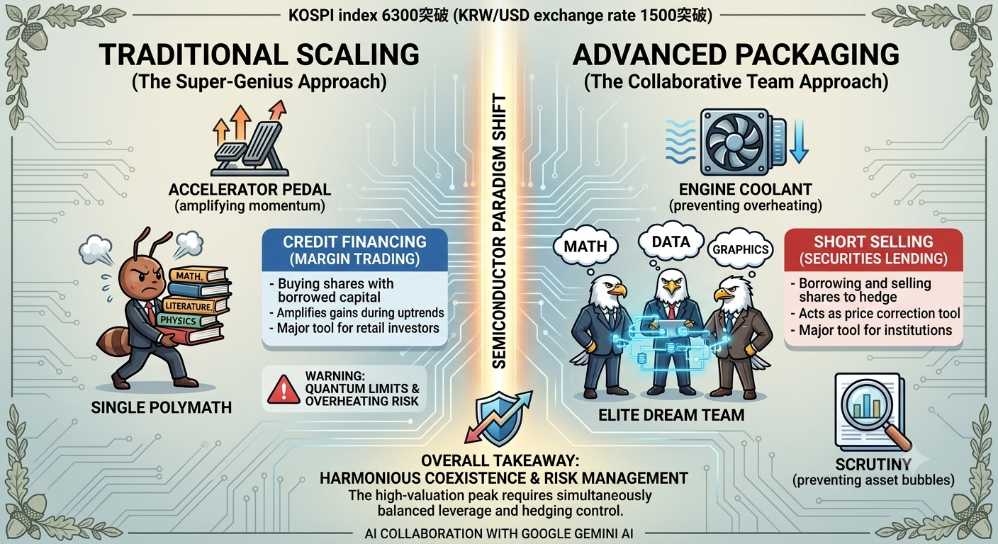
2) Scaling as “Nurturing a Single Polymath”
Traditional scaling attempts to train a single individual to achieve perfection across every academic subject—mathematics, literature, and physics alike. While a single genius can execute tasks rapidly without internal communication delays, overloading them with too much information causes severe burnout. In silicon design, forcing every function onto a single micro-scaled die leads to excessive heat generation, electrical current leakage, and high manufacturing defect rates.
3) Packaging as “Assembling an Elite Dream Team”
Advanced packaging gathers distinct experts—a mathematics specialist, a data engineer, and a graphics wizard—and integrates them into a cohesive unit. Provided the communication links between team members are fast and reliable, this collective team accomplishes far more complex projects than any single individual. This modular approach underpins the modern chiplet architecture favored by leading tech companies today.
3. Why Advanced Packaging Has Taken Center Stage
For decades, aggressive scaling alone guaranteed generational performance gains. Today, economic and physical realities have elevated packaging into a primary strategic priority.
- Physical Limits of Silicon: As node dimensions shrink to the level of individual atoms, physical phenomena like electron tunneling cause power leakage and thermal throttling. Shrinking components further no longer yields proportional gains in energy efficiency or speed.
- Escalating Capital Expenditures: Building state-of-the-art fabrication plants equipped with Extreme Ultraviolet (EUV) lithography machines requires tens of billions of dollars in capital investment. Advanced packaging offers a cost-effective alternative, enabling dramatic performance gains by linking mature, cost-effective nodes with cutting-edge logic dies rather than forcing every component onto an expensive, bleeding-edge process node.
4. Key Semiconductor Players Driving Innovation
The global semiconductor industry is locked in intense competition to master both scaling and advanced packaging integration.
- TSMC (Taiwan): Widely recognized as the industry leader in advanced packaging solutions, such as CoWoS (Chip-on-Wafer-on-Substrate). TSMC manufactures and packages the flagship AI accelerators used by NVIDIA and AMD, establishing a formidable competitive moat in the AI ecosystem.
- Samsung Electronics (South Korea): One of the few global companies possessing end-to-end capabilities spanning memory manufacturing, foundry services, and advanced packaging. Samsung leverages this integrated structure to deliver High Bandwidth Memory (HBM) stacked directly alongside high-performance logic units.
- Intel (USA): Historically the dominant force in traditional node scaling, Intel has invested heavily in proprietary packaging technologies like Foveros (3D stacking) and glass substrates to re-establish leadership in next-generation enterprise and AI computing markets.
5. Structural Comparison Table
| Category | Scaling (Miniaturization) | Packaging (Integration) |
|---|---|---|
| Core Goal | Shrinking internal circuitry to maximize die density | Stacking and interconnecting multiple chips into a single package |
| Culinary Analogy | Hyper-precise ingredient knife skills | Artfully curated multi-course meal |
| Primary Advantage | Maximizes single-die performance and energy efficiency | Reduces manufacturing costs; allows modular, customized design |
| Key Challenge | Approaching quantum physics boundaries and severe thermal limits | Minimizing latency and heat transfer across inter-chip connections |
Conclusion: Key Takeaways
- The Architectural Shift: The semiconductor industry has transitioned from relying purely on single-die miniaturization to embracing multi-chip modular integration through advanced packaging.
- Economic and Physical Imperatives: Escalating lithography costs and quantum-level physical constraints make advanced packaging the most viable path forward for scaling AI processing power.
- Industry Implications: Foundries and chipmakers capable of mastering both node scaling and 2.5D/3D packaging techniques—such as TSMC, Samsung, and Intel—will define the future landscape of high-performance computing.