
In the past, manufacturing a semiconductor was much like carving an entire single-family home from a massive, solid block of stone. Today, that approach is shifting toward a LEGO-like modular system, where individual rooms—such as the living room, master bedroom, and kitchen—are fabricated separately and assembled into a complete structure. As the artificial intelligence era drives demand for increasingly complex, high-performance computing, traditional manufacturing methods have become prohibitively expensive and prone to high defect rates. Rather than attempting to build a single all-in-one super-robot in a single facility, it is vastly more efficient to source specialized components—such as arms, legs, and processing units—from best-in-class specialized manufacturers and assemble them with precision. This deep dive breaks down the key differences between the traditional Monolithic design and the game-changing Chiplet architecture.
1. Single Block vs. Modular Assembly: A Paradigm Shift in Design
Modern microchips pack billions of microscopic components onto tiny surfaces. As computing demands skyrocket, semiconductor engineers face a critical dilemma: simply scaling up the physical size of a single chip creates severe yield issues, where even a microscopic speck of dust during manufacturing can render an entire oversized silicon wafer useless.
Understanding the difference between Monolithic and Chiplet architectures is key to grasping the future of hardware computing:
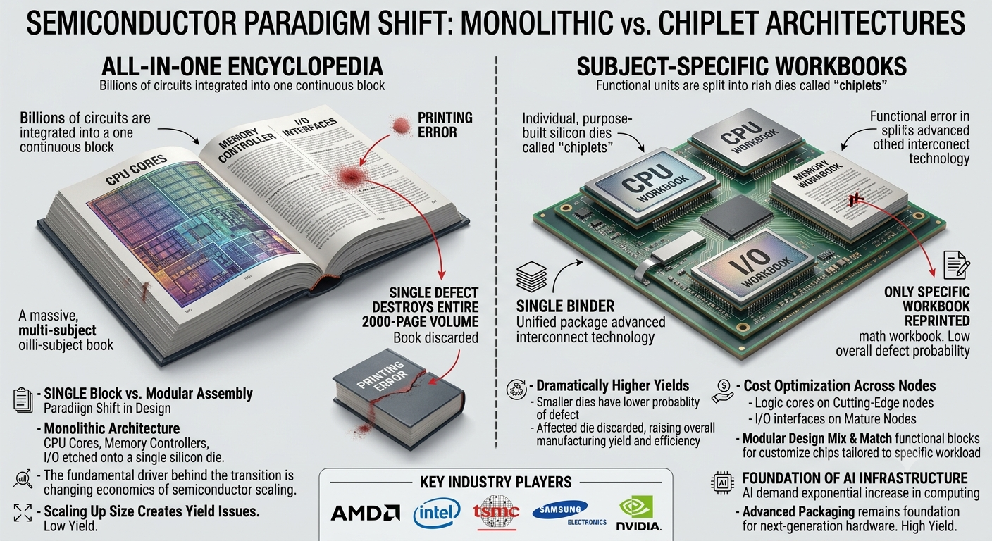
- Monolithic Architecture: All functional units (CPU cores, memory controllers, input/output interfaces) are etched onto a single, continuous silicon die. Think of it as preparing a massive single-dish roast. If one section gets burned or contaminated during cooking, the entire meal must be discarded.
- Chiplet Architecture: The monolithic chip is broken down into smaller, functional building blocks called “chiplets.” Each piece is manufactured independently—often using the most cost-effective manufacturing process for its specific function—and integrated into a single unified package via advanced interconnect technologies. This operates much like a modern meal kit: each pre-measured, quality-checked ingredient is prepared separately and brought together efficiently, eliminating waste.
2. Breaking Down the Terms and Analogies
Understanding the Etymology
- Monolithic: Derived from the Greek Mono (meaning “single”) and Lithos (meaning “stone”). In hardware design, it refers to a single, monolithic block of silicon housing every feature on one die.
- Chiplet: Combines Chip (a piece of semiconductor material) with the diminutive suffix -let (meaning “small”). It refers to miniature, purpose-built silicon dies designed to interoperate within a larger modular system.
Real-World Analogies for Easy Comprehension
Monolithic = The All-in-One Encyclopedia
Imagine printing an entire multi-subject encyclopedia as a single, massive 2,000-page volume. If a printing error occurs on page 1,400, the entire 2,000-page book must be discarded. As the volume grows thicker and more complex, maintaining flawless production quality across every page becomes nearly impossible.
Chiplet = Subject-Specific Workbooks
Instead of one giant volume, each subject—mathematics, history, literature—is printed as its own slender workbook. These separate workbooks are then organized into a single binder. If a printing error occurs in the math workbook, only that specific booklet is reprinted. Furthermore, each workbook can be produced by the specialized publisher best suited for that subject matter.
3. Why Is Chiplet Technology Becoming the Industry Standard?
The fundamental driver behind the transition to chiplet technology is the changing economics of semiconductor scaling.
- Dramatically Higher Yields: Manufacturing defects occur randomly across silicon wafers. On a large monolithic die, a single defect destroys the entire chip. Smaller chiplet dies have a significantly lower probability of containing a defect. When defects do occur, only the small affected die is discarded, raising overall manufacturing yields and efficiency.
- Cost Optimization Across Nodes: Not all semiconductor components require cutting-edge, expensive fabrication nodes (such as 3nm or 2nm processes). High-performance logic cores can be fabricated on costly, bleeding-edge nodes, while input/output interfaces or legacy power circuits can be built on mature, lower-cost nodes before being combined into a single package.
- Customizable Modular Design: Chiplets allow hardware vendors to mix and match standard functional blocks to create customized chips tailored to specific workload requirements without incurring the massive expense of designing a new monolithic chip from scratch.
4. Side-by-Side Comparison
5. Key Industry Players Driving the Modular Revolution
Several global semiconductor leaders are driving the commercial adoption of chiplet architectures:
- AMD: A pioneer in commercializing chiplet design. AMD proved the commercial viability of modular architectures with its Zen architecture Ryzen and EPYC processors, capturing significant market share.
- Intel: Utilizing its “Tile” methodology, Intel integrates chiplet technology into its client and data center processors, leveraging advanced 2.5D and 3D packaging capabilities like Foveros.
- TSMC: Provides the foundry infrastructure and advanced packaging technologies (such as CoWoS and InFO) required to bridge separate dies with ultra-dense interconnects.
- Samsung Electronics: Expanding its advanced packaging ecosystem to combine memory units, such as High Bandwidth Memory (HBM), with compute logic dies using next-generation interconnect solutions.
- NVIDIA: Implementing modular chiplet designs in its flagship AI processors, such as the Blackwell platform, to scale compute density beyond traditional single-die limitations.
Conclusion: Key Takeaways
- The End of Physical Limits: Traditional monolithic scaling is reaching its physical and financial boundaries. Building larger single dies is no longer economically sustainable for cutting-edge computing.
- Modular Efficiency: Chiplets solve the yield and cost dilemma by splitting large processors into smaller, modular dies that can be produced at higher success rates and assembled into a single functional unit.
- Cost and Flexibility: By combining cutting-edge manufacturing processes for core compute dies with mature, lower-cost processes for standard interfaces, hardware makers can deliver customized, high-performance silicon efficiently.
- The Foundation of AI Infrastructure: As artificial intelligence drives demand for exponential increases in compute capacity, advanced packaging and chiplet design will remain the primary architectural foundation for next-generation hardware.
AI Disclosure: Images and foundational research for this article were created in collaboration with Google Gemini AI. The final content was translated, rewritten, reviewed, and published by the author.