
In early computing history, computers operated as passive tools strictly executing pre-programmed user instructions. Today, artificial intelligence has evolved into an autonomous, highly adaptive cognitive infrastructure. Driving this technological transformation are two primary hardware components: the Graphics Processing Unit (GPU) and High Bandwidth Memory (HBM).
Think of this hardware architecture as a high-performance super-engine paired with an ultra-wide fuel delivery system. The GPU functions as the computational engine executing parallel calculations, while HBM acts as the specialized high-speed fuel line delivering vast amounts of data without interruption. As large language models expand, the economic and structural dynamic between processing and memory is shifting across the technology landscape.
1. The Master Chef and the Ultra-Fast Culinary Supply Chain
The capability of an artificial intelligence platform depends on processing speed and parallel data handling. Modern AI workloads divide these tasks between compute engines and memory bandwidth.
A GPU is an architecture optimized to execute thousands of simple mathematical operations simultaneously. However, even the fastest processor remains idle if input data arrives slowly. HBM addresses this challenge by providing thousands of microscopic physical interconnect channels that shuttle data directly to processing cores. Integrating a high-performance GPU with an advanced HBM supply chain creates a complete, high-throughput AI computing platform.
2. Real-World Analogies for Easy Comprehension
Etymology and Core Definitions
- GPU: Originally engineered to render complex 3D visual graphics, the GPU relies on thousands of compact cores designed to perform parallel arithmetic calculations concurrently, functioning as the primary computational workhorse for neural networks.
- HBM: Built by vertically stacking DRAM dies like a high-rise structure using Through-Silicon Vias (TSVs), HBM expands physical pin counts and bus widths to create high-speed data transfer routes.
Everyday Analogies
GPU = Thousands of Parallel Workers
Instead of relying on a single, highly specialized mathematician to solve one complex problem sequentially, a GPU deploys thousands of individual workers to execute basic arithmetic problems simultaneously. This architecture is suited for processing neural network parameter matrices, image recognition tasks, and natural language generation.
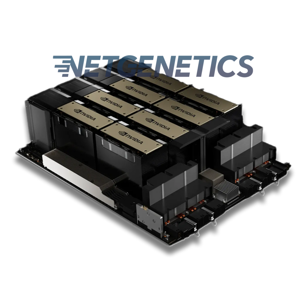
HBM = An Ultra-Wide Dedicated Transit Highway
Standard memory architecture functions like a narrow two-lane road where traffic easily congests. HBM expands that pathway into a multi-thousand-lane expressway, ensuring continuous data flow to the GPU compute cores without structural traffic delays.
3. System Imbalances: Understanding the Memory Bottleneck
Scenario A: Powerful GPU Performance with Limited HBM Bandwidth
- Processor Latency: The compute engine completes its mathematical operations in milliseconds, but narrow data lanes force processing cores to wait idle for incoming data batches.
- Hardware Underutilization: Purchasing expensive processing accelerators without sufficient memory bandwidth limits real-world compute output, running advanced hardware below its peak capacity.
Scenario B: Abundant HBM Bandwidth with Insufficient GPU Compute
- Calculation Stagnation: Data flows across wide memory channels, but an inadequate number of processing cores creates a backlog in execution queues.
- Energy Inefficiency: Keeping memory channels active without sufficient GPU compute resources consumes power while yielding sub-optimal throughput.
4. Architectural Innovations Overcoming the Memory Wall
To eliminate data transmission bottlenecks between GPUs and HBM modules, semiconductor manufacturers are implementing new hardware packaging and integration strategies:
2.5D / 3D Packaging
Mounts GPUs and HBM side-by-side on silicon interposers (CoWoS) or stacks HBM directly on logic dies to shorten interconnect distances.
PIM (Processing-In-Memory)
Embeds arithmetic logic units directly inside memory layers, reducing data movement energy consumption by up to 80%.
CXL Interconnects
Pools external memory resources into a unified, high-speed memory space to dynamically expand bandwidth capacity.
1) Advanced 2.5D and 3D Packaging
By placing GPU logic dies and HBM modules closely together on a silicon interposer—such as TSMC’s Chip-on-Wafer-on-Substrate (CoWoS)—manufacturers significantly shorten interconnect trace lengths. Emerging 3D integration techniques go further by stacking HBM directly on top of base logic dies, reducing physical latency and operational power consumption.
2) Processing-In-Memory (PIM)
PIM technology integrates execution units directly within individual DRAM layers. Rather than transferring massive datasets across external buses to the GPU for minor calculations, PIM enables the memory subsystem to process basic mathematical operations locally and transmit only the final computed output, reducing overall power consumption.
3) Compute Express Link (CXL)
CXL establishes an open, cache-coherent interconnect standard that pools disparate memory hardware across accelerators, host processors, and external modules. This allows system operators to expand available memory capacity dynamically beyond traditional physical motherboard limits.
5. Market Shifts: The Rise of Custom Silicon and Memory Economics
While NVIDIA maintains market dominance in high-performance discrete GPUs, major Cloud Service Providers (CSPs) are developing custom Application-Specific Integrated Circuits (ASICs)—such as Google’s TPU, Amazon’s Trainium, and Microsoft’s Maia—to optimize workload efficiency and reduce supply chain dependencies.
Concurrently, severe memory supply constraints and surging demand for stacked DRAM have led to sharp increases in HBM contract prices. In recent market cycles, memory manufacturers have seen revenue growth and profit margins rivaling traditional fabless GPU designers. This financial shift underscores a changing reality in AI hardware: high-density, high-bandwidth memory sub-systems have become as critical—and economically valuable—as the GPUs they supply.
6. Component Comparison Matrix
Conclusion: Key Takeaways
- Symbiotic Hardware Pairing: Peak AI infrastructure performance requires tight integration between GPU calculation engines and HBM data delivery pathways.
- Overcoming Bottlenecks: Advanced 2.5D/3D packaging, PIM architectures, and CXL memory pooling are essential strategies to bypass physical memory transfer limits.
- Shifting Economic Power: Soaring HBM prices and supply limitations have made high-bandwidth memory a dominant cost component, shifting profit margins across the semiconductor value chain.
- Diversification via Custom Silicon: Cloud providers are increasingly building custom ASICs to lower GPU procurement costs, while relying on advanced HBM integration to preserve system performance.
AI Disclosure: Images and foundational research for this article were created in collaboration with Google Gemini AI and ChatGPT. The final content was translated, rewritten, reviewed, and published by the author.